Op-Amp Gain and Offset Design with the HP-41C Programmable Calculator
May 26, 2009
This is a program I originally wrote for the HP-67 calculator, and then ported to the HP-41C series. This program is for designing offset-and-gain stages using a single operational amplifier. Such stages are often necessary to convert an input signal covering one range of voltages (e.g., 0.1V to 0.2V from a sensor) to an output signal covering a different range (e.g., 1.0 to 4.0V into an A/D converter).
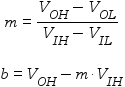
Mathematically, such a stage performs a linear transformation on the input voltage,
VOUT = m VIN + b
where m is the slope and b is the intercept or offset.
Given an input voltage range, VIL to VIH, and an output voltage range, VOL to VOH, the slope and offset are given by:
There are four main cases to consider, with different circuits for each, that are addressed by this program:
- Positive slope and offset (m > 0 and b > 0)
- Positive slope and negative offset (m > 0 and b < 0)
- Negative slope and positive offset (m < 0 and b > 0)
- Negative slope and offset (m < 0 and b < 0)
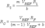
Positive Slope and Offset
A positive slope and offset stage is implemented by the following circuit:

Positive gain, positive offset amplifier
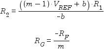
The designer must select values for R1 and RF, and then appropriate values for R2 and RG can be calculated using the following formulae:
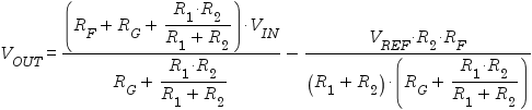
After determining theoretically ideal values for R2 and RG, real-world values can be chosen and the following formula applied to VIL and VIH to see the resulting values of VOL and VOH respectively:

This case is also used to handle the special case where b = 0 (postive gain with no offset). In such a case, the formula for R2 would result in dividing by zero, which means R2 is infinite. In other words, R2 and VREF are not needed. The value of R1 won’t matter then either, and can be replaced by a direct connection. The circuit reduces to:

Positive gain, zero offset amplifier
Positive Slope and Negative Offset
The following circuit implements a positive slope and negative offset stage:

Positive gain, negative offset amplifier
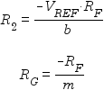
After choosing values for R1 and RF, values for R2 and RG can be be calculated using these formulae:
The following formula can then be used to determine the effect of real-world values of R2 and RG on the transformation:
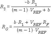
Negative Slope and Positive Offset
A negative slope and postive offset stage is implemented by the following circuit:

Negative gain, positive offset amplifier
Given values for R1 and RF, values for R2 and RG can be be calculated as follows:
The following formula can then be used to determine the effect of substituting real-world values of R2 and RG:
This case is also used to handle the special case where b = 0 (negative gain with no offset). As in case 1, the formula for R2 would involve division by zero, so R2 and VREF are not needed. The non-inverting input of the op-amp can be connected directly to ground, giving the following circuit:

Negative gain, zero offset amplifier
Negative Slope and Offset
The following circuit implements a negative slope and offset stage:

Negative gain, zero offset amplifier
This circuit has no R1, so it is only necessary to choose a value for RF, after which R2 and RG are given by:
The effect of using real-world values of R2 and RG can then be tested using this formula:
Limitations
Theoretically, the formulae presented here work perfectly well for gains between -1 and 1 (i.e. |m| < 1). However, many real-world op-amps are unstable in such cases. Instead, it will usually be necessary to design for a higher gain (|m| ≥ 1), with an attenuator on the input side. The design procedures for this are described on Texas Instruments’ Op Amp Gain and Offset Page.
Using the Program
First type in the program and save it, or read it from a previously recorded magnetic card. The card should be labelled as follows:
| OP-AMP GAIN AND OFFSET STAGE DESIGN | ||||
|---|---|---|---|---|
| VREF | VIL,VIH | VOL,VOH | ||
| →m,b | →CASE | R1,RF→R2,RG | R2,RG→VOL,VOH | |
Forward Solution: Finding R2 and RG
Consider the following example. A sensor has an output ranging from 0.5V to 0.7V, and we want to interface it to an A/D converter that is expecting an input between 1V and 4V. There is no reference voltage available other than the well regulated 5V supply voltage of the circuit. Use a 10kΩ resistor for R1, and 100kΩ for RF.
Follow these steps to solve the problem:
| Description | Keystrokes | Display |
|---|---|---|
| Use engineering notation | ENG 2 | 0.00 00 |
| Enter VREF | 5 a |
5.00 00 |
| Enter VIL and VIH | 0.5 ENTER 0.7 b |
500. -03 |
| Enter VOL and VOH | 1 ENTER 4 c |
1.00 00 |
| Compute slope m | A | 15.0 00 |
| Compute offset b | R/S | -6.50 00 |
| Determine case number | B | 2.00 00 |
| Enter R1 and RF, compute R2 | 10 EEx 3 ENTER 100 EEx 3 C |
1.02 03 |
| Compute RG | R/S | 6.21 03 |
Notes
It is not necessary to compute the slope and offset (by pressing A) before determining the case number. Likewise, it isn’t necessary to determine the case number (by pressing B) before computing resistor values (although you’ll want to know the case number in order to know which circuit to build). The program keeps track of which information is up to date, and will (re)compute anything that it needs that hasn’t already been computed.
Reverse Solution: Finding the Effect of R2 and RG on VOL and VOH
The closest available 5% resistor values for R2 and RG are 1kΩ and 6.2kΩ respectively. What effect does using these have on the solution? Follow these steps to find out:
| Description | Keystrokes | Display |
|---|---|---|
| Enter R2 and RG, compute VOL | 1 EEx 3 ENTER 6.2 EEx 3 D |
1.13 00 |
| Compute VOH | R/S | 4.15 00 |
This is within the A/D’s input range at the lower bound, but outside the range at the upper bound. What happens if we use the next available value for RG, 6.8kΩ, instead?
| Description | Keystrokes | Display |
|---|---|---|
| Enter R2 and RG, compute VOL | 1 EEx 3 ENTER 6.8 EEx 3 D |
1.09 00 |
| Compute VOH | R/S | 3.88 00 |
This is almost centered within the desired output range, and covers 93% of it.
The only remaining concern is how component tolerances might affect the solution. This can be analyzed by trying different combinations of R1, R2, RF, and RG representing resistors that are maximally out of tolerance (±5%) in each direction.
For example, to test the case where R1 and RF are 5% low and R2 and RG are 5% high, follow these steps:
| Description | Keystrokes | Display |
|---|---|---|
| Enter low R1 and RF, ignore computed R2 | 0.95 EEx 3 ENTER 95 EEx 3 C |
920. 00 |
| Enter high R2 and RG, compute VOL | 1.05 EEx 3 ENTER 7.14 EEx 3 D |
808. -03 |
| Compute VOH | R/S | 3.48 00 |
The results show that in this case, the lower limit of the output is out of range, meaning either a redesign is necessary, or tighter tolerance components are needed.
Cases where b = 0
In cases where the offset, b, is zero, the program will instead use b = 10-9 as the offset. This will avoid any division-by-zero errors. The program will then use case 1 (if m > 0) or case 3 (if m < 0) to compute the solution. In both cases, the computed value for R2 will be very large, typically around 109 times the value specified for R1. This indicates that R2 and VREF can be omitted, and that R1 can be replaced by a direct connection.
Program Listing
| Line | Instruction | Comments |
|---|---|---|
| 01♦ | LBL “GOFF” | |
| 02♦ | LBL a | Enter available reference voltage |
| 03 | STO 09 | |
| 04 | RTN | |
| 05♦ | LBL b | Enter VIL and VIH |
| 06 | STO 06 | Store VIH |
| 07 | x↔y | |
| 08 | STO 05 | Store VIL |
| 09 | CF 00 | Must recompute m and b |
| 10 | RTN | |
| 11♦ | LBL c | Enter VOL and VOH |
| 12 | STO 08 | Store VOH |
| 13 | x↔y | |
| 14 | STO 07 | Store VOL |
| 15 | CF 00 | Must recompute m and b |
| 16 | RTN | |
| 17♦ | LBL A | Compute transfer function slope (m) and intercept (b) |
| 18 | FS? 00 | Are m and b already up to date? |
| 19 | GTO 05 | |
| 20 | RCL 08 | Compute and store m = (VOH – VOL) ÷ (VIH – VIL) |
| 21 | RCL 07 | |
| 22 | − | |
| 23 | RCL 06 | |
| 24 | RCL 05 | |
| 25 | − | |
| 26 | ÷ | |
| 27 | STO 20 | |
| 28 | RCL 05 | Compute and store b = VOH – m VIL |
| 29 | × | |
| 30 | RCL 07 | |
| 31 | − | |
| 32 | CHS | |
| 33 | x≠0? | |
| 34 | GTO 07 | |
| 35 | 1 E-9 | Make sure b is never exactly 0; |
| 36♦ | LBL 07 | |
| 37 | STO 21 | |
| 38 | SF 00 | Stored m and b are now up to date |
| 39 | CF 01 | Must recompute case number now |
| 40♦ | LBL 05 | Display computed or already up-to-date m and b |
| 41 | RCL 20 | |
| 42 | RTN | Return, leaving m on stack |
| 43 | RCL 21 | Display b if user pressed R/S after return |
| 44 | RTN | |
| 45♦ | LBL B | Compute case number and store in I |
| 46 | XEQ A | Make sure m and b are up to date |
| 47 | FS? 01 | Is case number already up to date |
| 48 | GTO 08 | |
| 49 | x<0? | |
| 50 | GTO 06 | Handle cases where m < 0 |
| 51 | 1 | |
| 52 | STO 25 | |
| 53 | RCL 21 | |
| 54 | x<0? | |
| 55 | ISZ 25 | Case 2: m positive and b negative |
| 56 | GTO 08 | Case 1: m positive and b positive |
| 57♦ | LBL 06 | Cases where m is negative |
| 58 | 3 | |
| 59 | STO 25 | |
| 60 | RCL 21 | |
| 61 | x<0? | |
| 62 | ISZ 25 | Case 4: m negative and b negative |
| 63♦ | LBL 08 | Case 3: m negative and b positive |
| 64 | SF 01 | Case number is now up to date (or was already up to date) |
| 65 | RCL 25 | Display case number and return |
| 66 | RTN | |
| 67♦ | LBL C | Compute solution using appropriate case |
| 68 | STO 03 | Store RF |
| 69 | x↔y | |
| 70 | STO 01 | Store R1 |
| 71 | XEQ B | Get case number |
| 72 | GTO IND 25 | Branch to appropriate case |
| 73♦ | LBL 01 | Positive m and positive b |
| 74 | RCL 01 | Compute and store R2 = VREF R1 m ÷ b |
| 75 | RCL 09 | |
| 76 | × | |
| 77 | RCL 20 | |
| 78 | × | |
| 79 | RCL 21 | |
| 80 | ÷ | |
| 81 | STO 02 | |
| 82 | R/S | Display R2; 9.99e99 means “open circuit” |
| 83 | RCL 09 | Compute and store RG = VREF RF ÷ (VREF (m – 1) + b) |
| 84 | RCL 03 | |
| 85 | × | |
| 86 | XEQ 09 | Compute VREF (m – 1) + b |
| 87 | GTO 05 | Divide, store RG, and return, leaving RG on stack |
| 88♦ | LBL 02 | Positive m and negative b |
| 89 | RCL 01 | Compute and store R2 = –R1 b ÷ (VREF (m – 1) + b) |
| 90 | RCL 21 | |
| 91 | CHS | |
| 92 | × | |
| 93 | XEQ 09 | Compute VREF (m – 1) + b, leaving VREF (m – 1) in register 0 |
| 94 | ÷ | |
| 95 | STO 02 | |
| 96 | R/S | Display R2 |
| 97 | RCL 01 | Compute and store RG = (R1 b + VREF RF) ÷ (VREF (m – 1)) |
| 98 | RCL 21 | |
| 99 | × | |
| 100 | RCL 09 | |
| 101 | RCL 03 | |
| 102 | × | |
| 103 | + | |
| 104 | RCL 00 | Subroutine 9 left VREF (m – 1) in register 0 for us |
| 105 | GTO 05 | Divide, store RG, and return, leaving RG on stack |
| 106♦ | LBL 03 | Negative m and positive b |
| 107 | RCL 01 | Compute and store R2 = R1 (VREF (m – 1) + b) ÷ –b |
| 108 | XEQ 09 | Compute VREF (m – 1) + b |
| 109 | × | |
| 110 | RCL 21 | |
| 111 | CHS | |
| 112 | ÷ | |
| 113 | STO 02 | |
| 114 | R/S | Display R2 |
| 115 | RCL 03 | Compute and store RG = –RF ÷ m |
| 116 | CHS | |
| 117 | RCL 20 | |
| 118 | GTO 05 | Divide, store RG, and return, leaving RG on stack |
| 119♦ | LBL 04 | Negative m and negative b |
| 120 | RCL 09 | Compute and store R2 = VREF RF ÷ –b |
| 121 | RCL 03 | |
| 122 | × | |
| 123 | RCL 21 | |
| 124 | CHS | |
| 125 | ÷ | |
| 126 | STO 02 | |
| 127 | R/S | Display R2 |
| 128 | RCL 03 | Compute and store RG = RF ÷ m |
| 129 | RCL 20 | |
| 130 | CHS | |
| 131♦ | LBL 05 | Common code to compute y ÷ x and store in RG |
| 132 | ÷ | |
| 133 | STO 04 | |
| 134 | RTN | Return, leaving RG on stack |
| 135♦ | LBL 09 | Compute VREF (m – 1) + b, leaving VREF (m – 1) in register 0 |
| 136 | RCL 20 | |
| 137 | 1 | |
| 138 | − | |
| 139 | RCL 09 | |
| 140 | × | |
| 141 | STO 00 | Save VREF (m – 1) in register 0 for later |
| 142 | RCL 21 | |
| 143 | + | |
| 144 | RTN | |
| 145♦ | LBL D | Compute VOL,VOH using supplied R2,RG |
| 146 | STO 04 | Store RG |
| 147 | x↔y | |
| 148 | STO 02 | Store R2 |
| 149 | XEQ B | Get case number |
| 150 | RCL 05 | |
| 151 | XEQ IND 25 | Compute VOL from VIL |
| 152 | R/S | Display computed VOL |
| 153 | RCL 06 | |
| 154 | GTO IND 25 | Compute VOH from VIH |
| 155♦ | LBL 01 | Compute VOUT for positive m and positive b |
| 156 | RCL 02 | |
| 157 | × | |
| 158♦ | LBL 00 | Entry point to compute (x + VREF R1) (1 + RF ÷ RG) ÷ (R1 + R2) |
| 159 | RCL 09 | |
| 160 | RCL 01 | |
| 161 | × | |
| 162 | + | |
| 163 | RCL 03 | |
| 164 | RCL 04 | |
| 165 | ÷ | |
| 166 | 1 | |
| 167 | + | |
| 168 | × | |
| 169 | RCL 01 | |
| 170 | RCL 02 | |
| 171 | + | |
| 172 | ÷ | |
| 173 | RTN | |
| 174♦ | LBL 02 | Compute VOUT for positive m and negative b |
| 175 | RCL 01 | |
| 176 | 1/x | |
| 177 | RCL 02 | |
| 178 | 1/x | |
| 179 | + | |
| 180 | 1/x | |
| 181 | RCL 04 | |
| 182 | + | |
| 183 | STO 00 | Store RG + R1 R2 ÷ (R1 + R2) for later |
| 184 | RCL 03 | |
| 185 | + | |
| 186 | × | |
| 187 | RCL 00 | |
| 188 | ÷ | |
| 189 | RCL 09 | |
| 190 | RCL 02 | |
| 191 | × | |
| 192 | RCL 03 | |
| 193 | × | |
| 194 | RCL 01 | |
| 195 | RCL 02 | |
| 196 | + | |
| 197 | RCL 00 | |
| 198 | × | |
| 199 | ÷ | |
| 200 | − | |
| 201 | RTN | |
| 202♦ | LBL 03 | Compute VOUT for negative m and positive b |
| 203 | 0 | |
| 204 | XEQ 00 | Compute (VREF R1) (1 + RF ÷ RG) ÷ (R1 + R2) |
| 205 | GTO 09 | Subtract VIN RF ÷ RG |
| 206♦ | LBL 04 | Compute VOUT for negative m and negative b |
| 207 | RCL 09 | |
| 208 | RCL 03 | |
| 209 | × | |
| 210 | RCL 02 | |
| 211 | ÷ | |
| 212 | CHS | |
| 213♦ | LBL 09 | Entry point to compute x – y RF ÷ RG |
| 214 | x↔y | |
| 215 | RCL 03 | |
| 216 | × | |
| 217 | RCL 04 | |
| 218 | ÷ | |
| 219 | − | |
| 220 | RTN |
Two interesting aspects of this program are its use of indirect addressing for branching to the forward and reverse solution subroutines for each of the four cases, and its use of repeated labels.
The forward solution for each of the four slope/offset cases is implemented by a sequence of instructions starting with the label corresponding to the case number (1 to 4). When the user presses C, the case number is computed if necessary, and a GTO (i) instruction then branches to the appropriate case.
Similarly, the reverse solution for each case is also labeled according to the case number. When the user presses D, VIL is recalled to the stack, after which a GSB (i) instruction causes VOL to be calculated. Then VIH is recalled, and GTO (i) is used to calculate VOH and then return.
So, there are two each of LBL 1 through LBL 4. This works because the HP-41C/CV/CX (and other vintage HP calculators) search forwards from the current step for the matching label. Thus the GTO (i) in step 73 will branch to the appropriate forward solution, and the GSB (i) in step 152 and GTO (i) in step 155 will branch to the appropriate reverse solution.
This program also makes use of many small subroutines to compute sub-expressions common to multiple solutions. Since there were not enough labels for all the subroutines needed, the same labels were used more than once. Had this not been done, the same sequence of steps would have been repeated several times, and the program would not have fit into the calculator’s 224 step memory.
Registers and Flags
| Register | Use |
|---|---|
| 00 | Temporary register |
| 01 | R1 (Ohms) |
| 02 | R2 (Ohms) |
| 03 | RF (Ohms) |
| 04 | RG (Ohms) |
| 05,06 | VIL and VIH, input voltage range |
| 07,08 | VOL and VOH, output voltage range |
| 09 | VREF |
| 11 | m, slope of transfer function |
| 12 | b, intercept of transfer function |
| 10 | Case number (1,2,3,4) |
| Flag | Meaning |
|---|---|
| 00 | m and b are up to date |
| 01 | Case number is up to date |
Revision History
2009-May-26 — Initial release.
![]()
![]()
![]()
![]()
![]()
![]()
![]()
![]()
![]()
![]()
Related Articles
If you've found this article useful, you may also be interested in:
- Op-Amp Oscillator Design with the HP-41C Programmable Calculator
- Low-Sensitivity Sallen-Key Filter Design with the HP-41C Programmable Calculator
- Low-Sensitivity Sallen-Key Filter Design with the HP-67 Programmable Calculator
- Op-Amp Gain and Offset Design with the HP-67 Programmable Calculator
- Op-Amp Oscillator Design with the HP-67 Programmable Calculator
- Resistor Network Solver for the HP-67 Programmable Calculator
- A Matrix Multi-Tool for the HP 35s Programmable Calculator
- Curve Fitting for the HP 35s Programmable Calculator

If you've found this article useful, consider leaving a donation in Stefan's memory to help support stefanv.com
Disclaimer: Although every effort has been made to ensure accuracy and reliability, the information on this web page is presented without warranty of any kind, and Stefan Vorkoetter assumes no liability for direct or consequential damages caused by its use. It is up to you, the reader, to determine the suitability of, and assume responsibility for, the use of this information. Links to Amazon.com merchandise are provided in association with Amazon.com. Links to eBay searches are provided in association with the eBay partner network.
Copyright: All materials on this web site, including the text, images, and mark-up, are Copyright © 2026 by Stefan Vorkoetter unless otherwise noted. All rights reserved. Unauthorized duplication prohibited. You may link to this site or pages within it, but you may not link directly to images on this site, and you may not copy any material from this site to another web site or other publication without express written permission. You may make copies for your own personal use.